Semicon 2.0 applications open for chip equipment, fabs and packaging projects
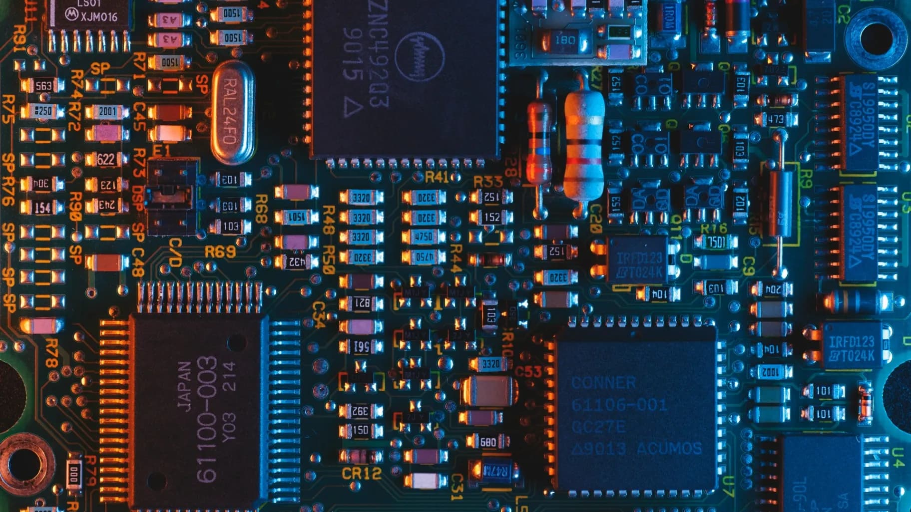
Semiconductor Chip
Union Minister for Electronics and Information Technology Ashwini Vaishnaw launched the Semicon 2.0 web application portal on November 6, 2026, opening applications for three parts of India’s semiconductor programme.
According to the Ministry of Electronics and Information Technology’s announcement, applicants can submit proposals under Pillar 2, for semiconductor machines and materials; Pillar 3, for additional fabrication plants, known as fabs; and Pillar 4, for assembly, testing and packaging facilities. The announcement does not say that applications are open under the programme’s other three pillars.
How to apply: Organisations considering a project can start at the India Semiconductor Mission’s official website and follow its Semicon 2.0 application link. They should select the pillar that matches their proposed project and read its current guidelines and eligibility requirements before submitting an application. This portal is for semiconductor project proposals; it is not visitor registration for a SEMICON India exhibition.

Separately, the ministry announced 12 approvals under the Electronics Components Manufacturing Scheme. These projects cover products such as printed circuit boards, copper foil and battery materials. The government estimates they could bring ₹7,503 crore in investment and 7,127 direct jobs. Those are projected outcomes, not investment or employment already delivered.
The distinction matters: the 12 newly approved applications belong to the electronics components scheme, while the portal opened on November 6 accepts proposals under Semicon 2.0.